English
 Español
 Português
 Pусский
 Français
 Deutsch
 日本語
日本語 한국어
한국어 Italiano
 عربى
عربى
Exploring TFT LCD display principle
<What is LCD>
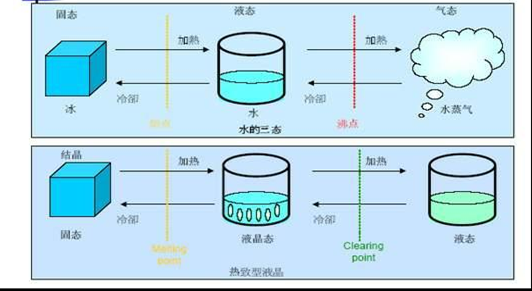
We generally think that objects have three states: solid, liquid, and gaseous. In fact, this is only for water. There are some organic and chemical substances, and the state between solid and liquid is the liquid crystal state, as shown in the following:
<TFT LCD display principle>
a: background
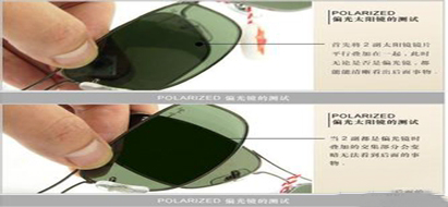
When the angles of two polarized fences are perpendicular to each other, light cannot pass through at all. Figure (6) is a test done with polarized sunglasses.
b:TFT LCD display principle
The liquid crystal display(LCD display) is completed by taking advantage of the characteristics of polarizing plates. The vertical polarizing plates between the upper and lower fences are filled with liquid crystals. The electric field is used to control the rotation of the liquid crystal branches to change the direction of light. In this way, different electric field sizes will form different colors, as shown in Figure (7).
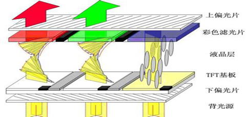
b-1: When no electrode is added, when the incident light passes through the polarizing plate (polarizer) below, a unidirectional light wave will remain. When passing through the liquid crystal molecules, the liquid crystal molecules rotate a total of 90 degrees. , so when the light wave reaches the upper polarizing plate, the polarization direction of the light wave turns exactly 90 degrees. The angles of the lower polarizing plate and the upper polarizing plate are exactly 90 degrees different. So the light can pass through smoothly. If the light hits the red filter, it will appear red. The effect is shown in the first two pictures in Figure (7).
b-2: After adding the electrode (maximum electrode), the liquid crystal molecules stand up under the influence of the electric field. The light path does not change, and the light cannot pass through the upper polarizing plate, and it cannot be displayed, as shown in Figure (7) LCD underneath the blue filter.
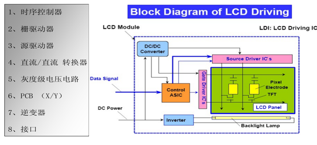
c: TFT-LCD drive circuit.
In order to display arbitrary graphics, TFT-LCD displays a progressive scan matrix arranged with m×n points. When designing a drive circuit, you must first consider that liquid crystal electrolysis will cause the liquid crystal material to deteriorate. To ensure longevity, AC drive is generally used. The driving modes that have been formed include: voltage selection mode, ramp mode, DAC mode and analog mode, etc. Since TFT-LCD is mainly used in notebook computers, the drive circuit is roughly divided into: signal control circuit, power circuit, gray scale voltage circuit, common electrode drive circuit, data line drive circuit and addressing line drive circuit (gate drive IC). The main functions of the above-mentioned drive circuit are: the signal control circuit supplies digital signals, control signals and clock signals to the digital IC, and supplies the control signals and clock signals to the gate drive IC; the power circuit supplies the required power voltage to the digital IC and gate Driving IC; the gray voltage circuit supplies each of the 10 gray voltages generated by the digital driving circuit to the data drive; the common electrode driving circuit supplies the common voltage to the shared electrode relative to the pixel electrode; the data line driving circuit supplies the signal control circuit Each 6-bit display data and clock signal of the RGB signal are latched in timing sequence and transferred internally. Then the display data is converted into an analog signal by a 6-bit DA converter, and then converted into an impedance by the output circuit and supplied to the LCD screen. Data line; the gate drive circuit converts the clock signal sent from the signal control circuit through the shift register conversion action, switches the output circuit to ON/OFF voltage, and adds it to the LCD screen in sequence. Finally, the drive circuit is assembled on the TAB (automatic welding flexible circuit board) and connected to the LCD display using ACF (anisotropic conductive film) and TCP (drive circuit flexible tape).
d:TFT-LCD working principle
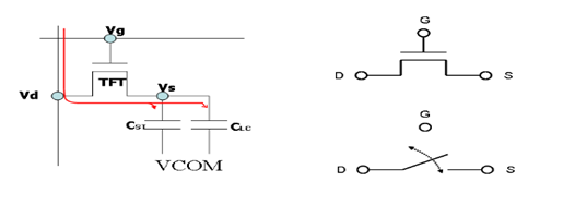
First, the display principle is introduced. The principle of liquid crystal display screen is based on the characteristic that the light transmittance of liquid crystal changes with the magnitude of the voltage applied to it. When the light passes through the upper polarizer, it becomes linearly polarized light. The polarization direction is consistent with the vibration direction of the polarizer, and is consistent with the arrangement order of liquid crystal molecules on the upper and lower glass substrates. When light passes through the liquid crystal layer, the linearly polarized light is decomposed into two beams of light due to refraction by the liquid crystal. And because the two beams of light propagate at different speeds (with the same phase), when the two beams of light are combined, the vibration direction of the vibrating light will inevitably change. Light passing through the liquid crystal layer is gradually distorted. When the light reaches the lower polarizer, its optical axis vibration direction is twisted by 90 degrees and remains consistent with the vibration direction of the lower polarizer. In this way, the light passes through the lower polarizer to form a bright field. After applying voltage, the liquid crystal is oriented under the action of the electric field and the distortion disappears. At this time, the linearly polarized light that passes through the upper polarizer no longer rotates in the liquid crystal layer and cannot pass through the lower polarizer to form a dark field. It can be seen that the liquid crystal itself does not emit light and can be displayed under the modulation of an external light source. During the entire display process, the liquid crystal acts as a voltage-controlled light valve. The working principle of TFT-LCD can be briefly described as: when the gate forward voltage is greater than the applied voltage, the drain-source electrode is turned on, and when the gate forward voltage is equal to 0 or negative voltage, the drain-source electrode is turned off. The drain electrode is connected to the ITO pixel electrode, the source electrode is connected to the source line (column electrode), and the gate electrode is connected to the gate line (row electrode). This is how TFT-LCD screen simply works.
F: Commonly used liquid crystal structures
F-1: The so-called NW (Normally white)
NW means that when we apply no voltage to the LCD panel, the panel we see is a bright picture, so it is called normally white. Another type, when no voltage is applied to the LCD panel, the panel cannot transmit light and looks black, which is called NB (Normally black)
c-2:Why are there these two structures?Mainly for different application environments. Generally, desktop computers or notebook computers are mostly configured with NW. This is because of the usage environment of general computer software. You will find that the entire screen is mostly bright spots, which means that computer software is mostly used with black text on a white background. Since the bright spots account for the majority, it is of course more convenient to use NW, and because the bright spots of NW do not require voltage, it will save more power on average.
On the contrary, most of the application environments of NB are applications where the display screen is black.
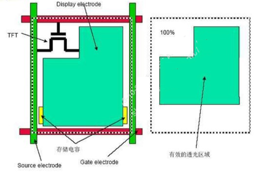
<Structure diagram of LCD single pixel>
a: Structure of LCD section:
b:Principle of action
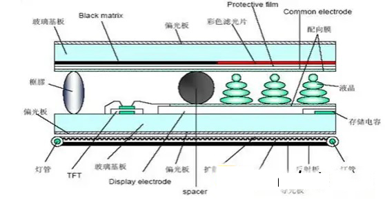
TFT LCD (thin film transistor liquid crystal display), the liquid crystal display requires voltage control to generate gray scale. TFT uses thin film transistors to generate voltage to control the display of liquid crystal steering. Judging from the cross-sectional structure diagram in Figure (8), when liquid crystal is sandwiched between the upper and lower layers of glass, a parallel plate capacitor will be formed, which we call CLC (capacitor of liquid crystal). Its size is about 0.1pF, but In practical applications, this capacitor cannot maintain the voltage until the next time the screen data is updated. That is to say, when the TFT charges this capacitor, it cannot maintain the voltage until the next time the TFT charges this point. When charging. (With a general screen update frequency of 60Hz, it needs to be maintained for about 16ms.) In this way, if the voltage changes, the gray scale displayed will be incorrect. Therefore, generally in the design of the panel, it will be Add a storage capacitor CS (storage capacitor is about 0.5pF) so that the charged voltage can be maintained until the next time the screen is updated. But to be precise, the TFT itself grown on the glass is just a transistor. switch. Its main job is to determine whether the voltage on the LCD source driver should be charged to this point. As for how high the voltage should be charged to this point in order to display what kind of gray scale. It is all determined by the external LCD source It's up to the driver to decide.
c: Sealant and spacer:
There are two structural components: frame glue and spacer. The purpose of frame glue is to allow the upper and lower layers of glass in the LCD panel to adhere tightly, and to provide a barrier between the liquid crystal molecules in the panel and the outside world, so the frame glue is just as its name suggests. , which surrounds the panel and limits the liquid crystal molecules within the panel. The spacer mainly provides support for the upper and lower layers of glass. It must be evenly distributed on the glass substrate, otherwise uneven distribution will cause some spacers to gather together. , On the contrary, it will hinder the passage of light, and it will not be able to maintain the appropriate gap (gap) between the upper and lower pieces of glass, which will cause uneven distribution of the electric field, thereby affecting the grayscale performance of the liquid crystal.
<LCD under a magnifying glass>
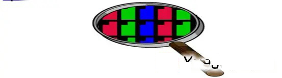
a: The structure of each pixel
The LCD panel under the magnifying glass is as shown in Figure (9). Each pixel is composed of three sub-primary colors: "red", "blue", and "green" (this is the so-called three primary colors. That is to say, using these three colors). We divide the three colors of RGB into three independent points, each with different gray scale changes, and then regard the three adjacent RGB display points as a basic unit of display, that is, pixel. Then this pixel, You can have different color changes. (Then for a display screen that requires a resolution of 1024*768, we only need to make the flat panel display have 1024*768 pixels,) and this screen can be displayed correctly.
b: opening rate
A very important parameter in an LCD display is brightness, and the most important factor that determines brightness is the aperture ratio. The aperture ratio is the proportion of the effective area through which light can pass. The black part between each RGB point is called the Black matrix. If we look back at the picture (9), we can find that the black matrix is mainly used to cover the parts that are not intended to transmit light. For example, some ITO The wiring, or the Cr/Al wiring, or the TFT part. This is why in Figure (9), each RGB highlight does not look rectangular, and there is also a piece of black in its upper left corner. The part covered by the matrix, this black missing corner is the location of the TFT.
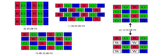
<Common filter arrangements>
<Pixel of the TFT LCD>
a: Pixel principle
Each pixel on the LCD panel is divided into three colors: red, green, and blue. RGB is the so-called three primary colors. These three colors can be used to mix various colors. We divide the three colors of RGB into three independent points. Each has different gray scale changes, and then the three adjacent RGB display points are regarded as a basic unit of display, which is a pixel. This pixel can have different color changes.
b: color depth
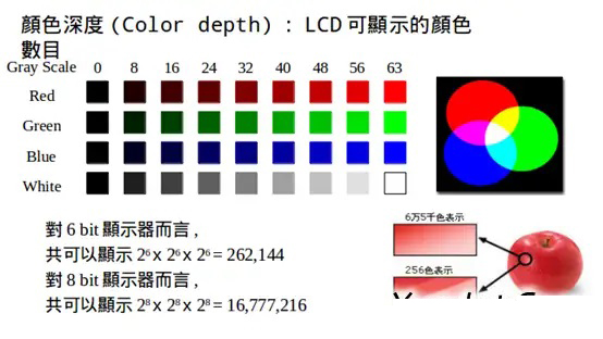
normal Color
256 Color 8(R)*8(G)*4(B)=256 Color
High Color
65536Coloe32(R)*64(G)*32(B)=65536 Color
Full Color
64(R)*64(G)*64(B)=262144 Color
True Color
256(R)*256(G)*256(B)=16777216 Color
<LCD internal circuit>
a: Structure diagram
b: The main parts that drive TFT work are as follows:
1. Source driver is responsible for power supply.
2. Gate driver is responsible for opening and closing.
3. Timing control circuit, responsible for controlling the gate driver
4. Gray scale and gamma control circuit
a: The general structure of the entire panel
From Figure (13) we can see the equivalent circuit of the entire panel, in which each TFT is connected in parallel with two capacitors (representing a display point. A basic display unit pixel requires three such displays The points represent the three primary colors of RGB respectively. For a TFT_LCD with a resolution of 1024*768, a total of 1024*768*3 such points are needed)
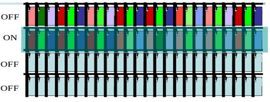
b: Display steps
As shown in the figure, the waveform sent by the gate driver turns on the TFTs of each row in sequence, so that the entire row of source drivers can charge the entire row of display points to their respective required voltages to display different gray levels. When When this row is fully charged, the gate driver turns off the voltage, and then the gate driver on the next row turns on the voltage, and then the same row of source drivers charge and discharge the display points on the next row. In this order, when the charge is Once the display point of the last row is finished, go back and start charging from the first row.
b-1:Illustration
Open the first row first and close the others.
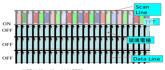
Then close the first row, the voltage has been fixed, and the solid color has been fixed, then open the second row, close the rest, and so on.
Because liquid crystal molecules also have a characteristic, they cannot always be fixed at a certain voltage. Otherwise, over time, even if you cancel the voltage, the liquid crystal molecules will no longer be able to rotate in response to changes in the electric field due to the destruction of their characteristics. To form different gray scales. Therefore, every once in a while, the voltage must be restored to its original state to avoid damaging the characteristics of the liquid crystal molecules.
<Backlight>
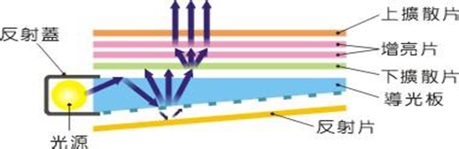
Most of the TFT type LCDs used in mobile phones use LED as the light source. There are three methods of backlighting on Qualcomm mobile phones:
1. PWM mode, controls the current size according to the duty cycle of the output square wave
2. One-line pulse mode, controls the output current according to the logic connection of the input square wave
3. DCS mode, with LCD feedback to the backlight control chip to control the output current.
Generally, there is a backlight control chip on mobile phones to boost the voltage and control the current. Take the backlight chip TPS61161 on the 8x25 as an example (other backlight chips are similar)
TPS61161 connection method:
CTRL needs to be connected to the GPIO on the platform or the GPIO on the PMIC.
This chip is used in both PWM mode and one-line pulse mode. The working mode is as follows:
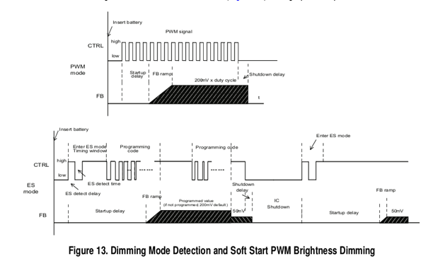
In the picture above, the upper part is the PWM mode. The control is directly connected to the backlight chip by the GPIO. One thing to note is that the PWM mode is generally directly controlled by the PMIC because if the AP control is used, the system load is heavy. The PWM waveform will be distorted. The lower part is the one-line pulse mode input. There needs to be a logic to trigger the one-line pulse mode.
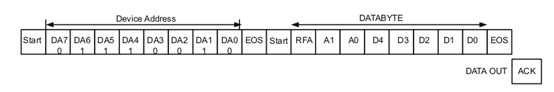
The data format is as follows:
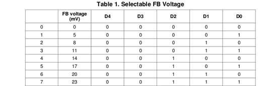
The current values corresponding to the data are as follows (only part of the current values are given)
In DCS mode, the LCD itself can support CABC or LABC function
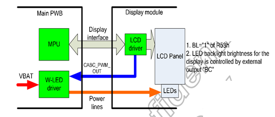
The principle is as shown in the figure. The platform uses mipi dcs command to control the CABC function. The LCD register is
51H (default backlight brightness 0 ~ 255)
53 H (open closed)
55H (mode defined differently by different manufacturers) backlight
The platform sends 51H 53H 55H to the LCD panel through the mipi package. The LCD panel calculates its own appropriate backlight value based on its own image and the backlight value sent by the platform, and sends it out in the form of a PWM square wave through the pins on the LCD panel. Platform, there is a corresponding backlight chip on the platform that accepts the PWM wave. The backlight chip controls the voltage at both ends of the LED on the LCD panel according to the PWM waveform to control the backlight.
In DCS mode, there is a problem that the PWM frequency of the LCD output and the input frequency of the backlight chip are related. You need to pay attention to it when debugging. Generally, the PWM frequency output by the LCD is adjustable.
 Ashley Wu